Building a Synthesizer, 3
Breadboarding the VCO
- Introduction: The World of DIY Synthesizers
- 1: The mki x es.EDU DIY System
- 2: Building the Power Supply
- 3: Breadboarding the VCO
- 4: A Gentle Introduction to Op Amps
- 5: Building the VCO
- 6: The Logic Circuits Model of Computation
- 7: Building the Mixer
- 8: Building the Envelope Generator
- 9: A Field Guide to Oscillators
- 10: Building the VCA
- 11: Debugging Circuits and Software Debugging
- 12: Breadboarding the VCF
- 13: Building the VCF
- 14: Building the Sequencer
- Glossary and Electrical Connections
Having previously built the power supply, it’s now time to go on to building actual synth modules. Yay!
There doesn’t seem to be any proscribed order to build the mks x es.EDU modules in. But it makes sense to start with a Voltage Controlled Oscillator (VCO), so that the other modules will have some sound to modify when built, and the sawtooth/Pulse Width Modulation (PWM) VCO is the most generally useful oscillator in the series, so I started with that kit.
On Making Mistakes
I’m going to describe the whole build process, with a particular focus on the mistakes I made. This is partly to help others fix similar problems they might have, but mostly it’s because I think that this is where the real learning happens.
“Debugging is twice as hard as writing the code in the first place. Therefore, if you write the code as cleverly as possible, you are, by definition, not smart enough to debug it.” - Brian W. Kernighan
The quote above goes both ways. Debugging teaches you more about writing code than just reading correct code in a book. Likewise, making a mistake on a breadboard, and then finding and fixing that mistake, teaches you much more than just soldering a circuit together. When something doesn’t work and you have to find the problems with a continuity tester and an oscilloscope, that’s what helps you to really understand what is happening in the circuit, and how to find this information using tools such as a digital multimeter, an oscilloscope, and your brain.
Breadboarding
The heart of the kit, in my opinion, is breadboarding. This is what distinguishes the mks x es.EDU kits from many other DIY synth kits. In contrast to other kits, where you build a completed circuit from start to finish and then power it on, with breadboarding you build and evolve the circuit for the VCO, adding features as you go.
The breadboard constuction proceeds in several phases.
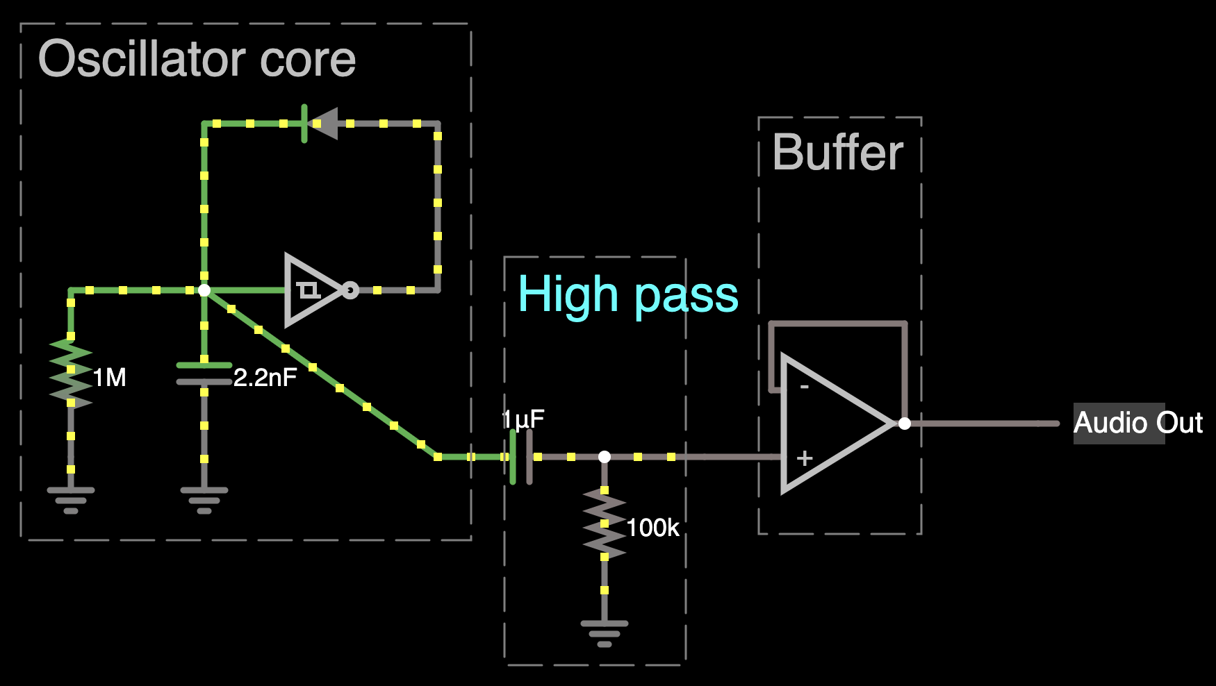
VCO Core
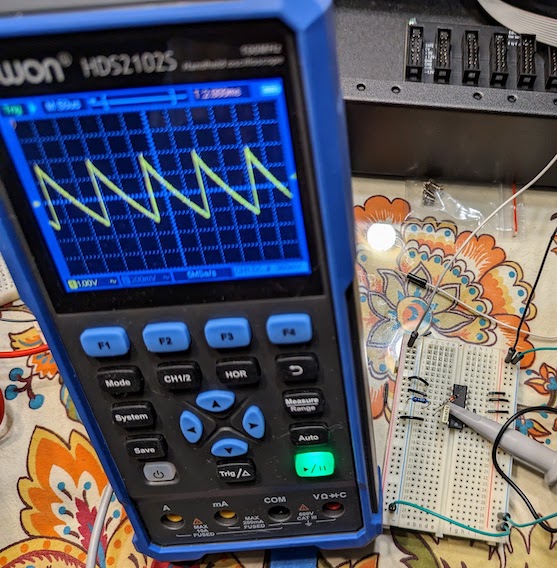
Building the oscillator core on the breadboard went easily, and the circuit worked the first time I tried it. This part “just worked.”
Note that the wave you can see in the image is sometimes called an “inverted” sawtooth: It shoots up to its maximum voltage and then falls slowly down to the minimum. This distinction (from a “ramp” or “regular” sawtooth wave, which grows slowly to its maximum and then falls quickly to the minimum) will be inaudible at audio frequencies, but it will be “different” if you’re using this oscillator as an LFO.
What frequency is the oscillator producing? Well, my oscilloscope tells me that the period of the period of the oscillation is 126.7 µS, so the frequency is the reciprocal of that, which is about 7893 Hz. This is approximately a B8 (a B on the 8th octave – about an octave above the range of a standard piano). So it’s a pretty high pitch!
One thing which I will not do in this series is to explain how the circuits work. For that you can read the very fine manual, where the author, Moritz Klein, does a better job than I could do explaining just that. Honestly, even if you have no intention of ever building these kits, the instructions are very useful reading. They are the clearest “starting from nothing, no knowledge assumed” explanations I’ve seen of audio circuitry.
Having said that, I do think it’s worth sharing this simulation of the oscillator core, because it’s super-helpful to be able to see how current moves inside the wires. The dots represent current, voltage is represented by color: higher voltages are green for positive, gray for neutral, and red for negative. (By default; use Options->Other Options…to change the colors if distinguishing red and green is challenging for you.)
Add Output Buffer
So now we have an oscillation, we’re done with the “VCO,” right? Not by a long stretch! The next step is to buffer the output so that you can connect headphones or another module and have the circuit keep working. Without this, the resistance of the headphones, etc., will change the frequency of vibration.
The circuit is quite simple, but I encountered a few issues building it.
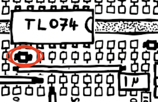
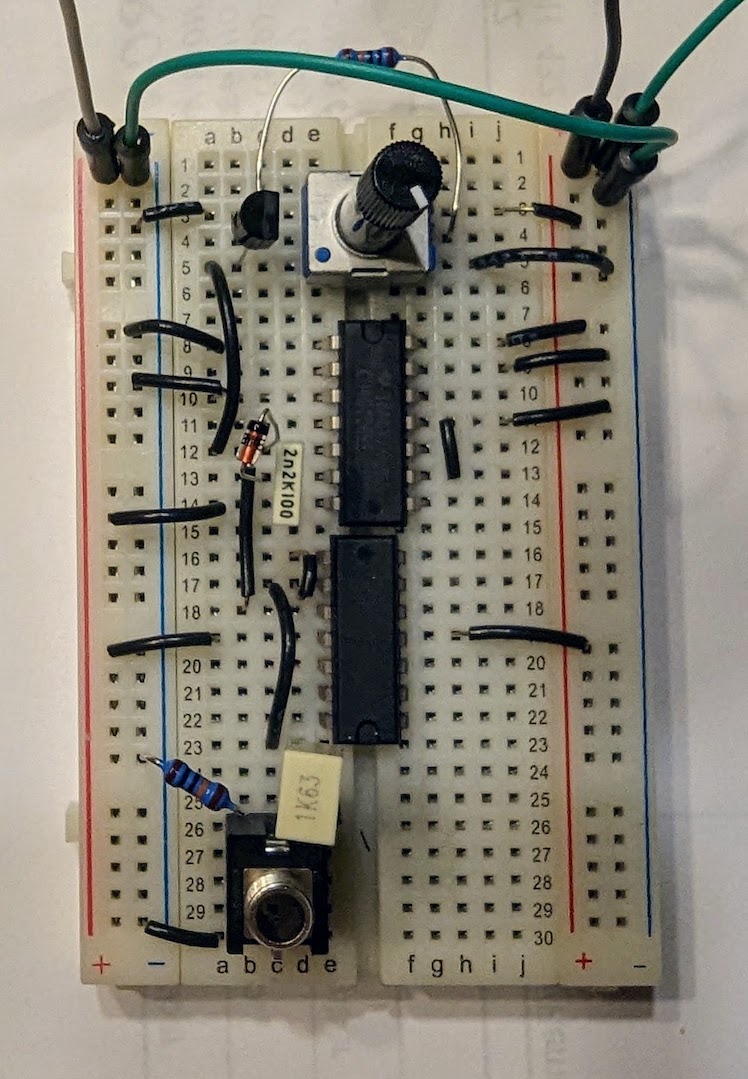
One minor frustration I had with the instructions for this kit concerned the breadboard assembly. The breadboarding instructions were primarily hand-drawn illustrations, and there was no accompanying schematic at each breadboard step. (There is a schematic for the whole VCO as assembled on the PC board.) I spent more time than I’d like to admit staring at the component circled in red at left, trying to figure out what it was, before I eventually realized it was just a very short wire!
A much bigger problem was that when I powered up the circuit the TL074 op amp chip became very hot. This tells me that power is going somewhere where it should not.
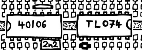
After a couple of minutes staring at the illustration, it traspired that I had installed the TL074 op amp chip upside down. It turns out I’m not the first to make this mistake! It’s a very easy mistake to make because the instructions are confusing. The two ICs are oriented differently on the breadboard (and probably need to be because of the locations of their power pins), and this is not called out in the instructions.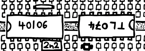
Worse, the TL074 is pictured incorrectly in the instructions! The text is depicted upside down. Above and to the right is the actual diagram from the instructions showing the IC text printed in the inverse of how it actually appears on the chip, and below that is my suggestion for how the diagram could be changed to clarify the actual way the chips could be installed.
Also, a further warning, just because the instructions seem to be going out of their way to confuse you on this point: The orientation of the two ICs is different in the breadboard layout vs. the PC board layout. All I can say is to double and triple-check the orientations vs. the specific step you are building at every step before turning on power, because they are not always the same, and getting it wrong means a cooked op-amp chip.
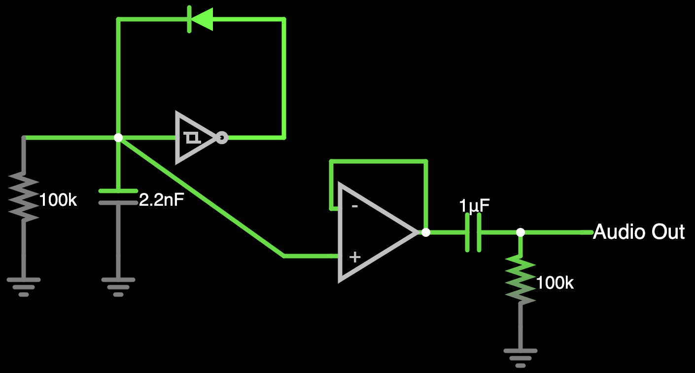
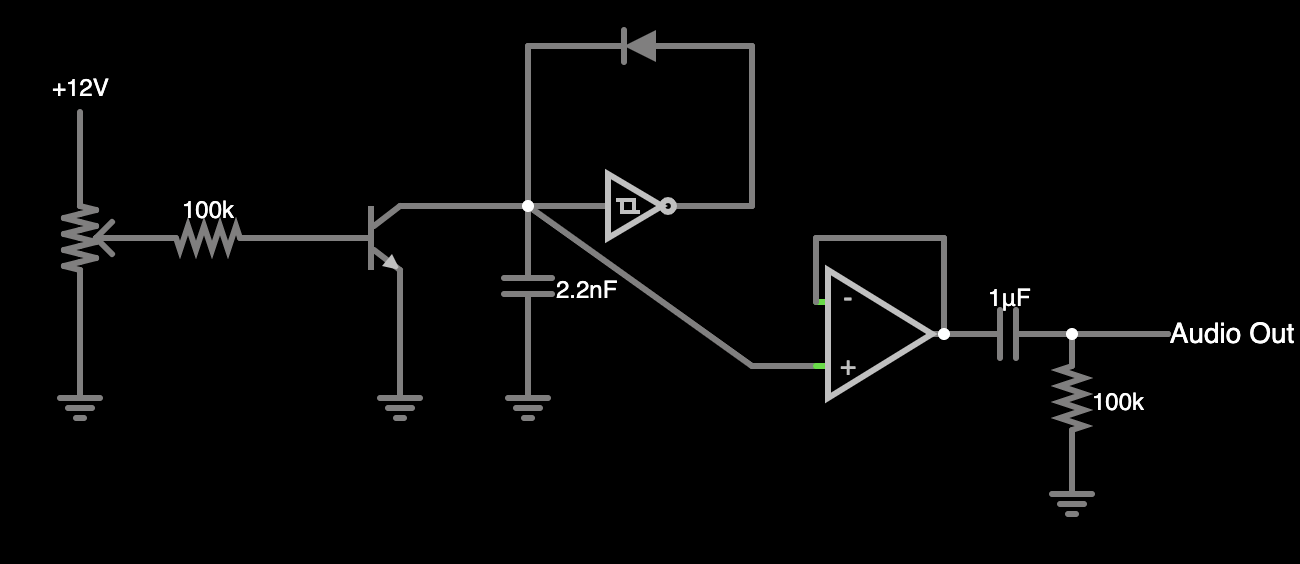
So I “borrowed” another TL074 from a different kit installed the chip correctly, and the circuit worked. I could measure the signal with my oscilliscope, which looked exactly like it did without the buffer, only without the DC offset. The instructions say to:
Plug some cheap headphones into the audio jack socket, and you should be able to hear a very high-pitched tone.
When I plugged my headphones into the jack I heard… mostly a low-frequency (5-10 Hz) clicking sound. After… a lot of debugging, I found that I had connected the wire which runs from the output of the op amp to the 1 µF capacitor just above the headphone jack incorrectly. I had the wire running to pin 10, the + input of the op amp, instead of pin 8, the output. Correcting this wire fixed the click, and I could hear the correct oscillation.
Let me spell this out with schematics, since it seems like others have had this problem:
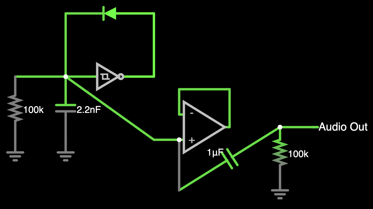
The schematics make my mistake super-clear! Whereas if you look at the actual breadboard (see the photo below), or the illustrations in the manual, it’s a lot less clear what is happening in the circuit. So I spent a fair amount of time drawing schematics of the breadboard experiments which followed. I hope you find them useful!
After working through all of these problems, I think that these mistakes, which were mostly mine, are exactly what I wanted from this whole project. The chance to screw up and then find the problems. This is, in my opinion, the best way to learn. You don’t get this kind of knowledge from a kit where you just solder chips onto a board and then you’re done. It’s wonderful!
(Note that the audio output is somewhat loud. If your headphones don’t have a volume control on them, I’d recommend keeping them off of your ears, at least at first.)
Digression: An Optimization?
The VCO at this point has essentially three sub-circuits, identifed below:
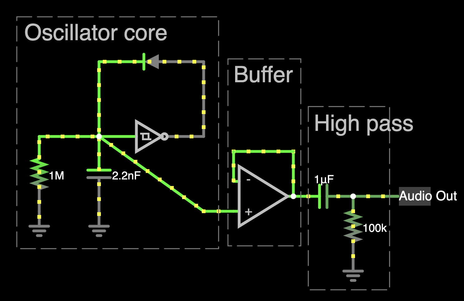
The oscillator core emits a sawtooth wave ranging from about 1.7 to 7.2V. This is well within the range of the op amp, but it’s not centered at 0. The DC (passive high pass) filter will center the oscillation around 0. I wondered if it would make more sense to switch the order? My thought had been that putting the DC filter before the buffer would result in the oscillator’s voltage range being more centered in the op amp’s range.
Since I find it easier to think in schematics than in board layout, I first modeled this in the simulator, thinking that I would try it on my breadboard when I was happy with the result. It’s worth noting that the simulator is not perfect, and some things work in real life which look strange in the simulator. But in this case my “improved” circuit doesn’t work at all, and I could immediately see why:
Instead of being two distinct sub-circuits separated by the buffer, the resistors and capacitors from the oscillator core and the passive high-pass filter are now a combined impedance, which breaks both sub-circuits! The oscillator now runs at the wrong rate, and the DC filtering doesn’t work at all. So much for that idea!
Changing the Frequency with a Potentiometer
Next, we experiment with changing the frequency of oscillation by substituting different values for the capacitor and the resistor in the oscillator core, which does indeed change the pitch of the tone that’s generated. Then we substitute a transistor for the resistor, which allows us to have a variable pitch by using a potentiometer connected to the transistor’s base. This potentiometer will eventually become the tuning knob.
The only real problem in this phase of the build was mounting the potentiometer to the breadboard; the pot I was given in the kit was much bigger than the pot drawn on the assembly diagram. I found a way to make it work (see below).
I find it helpful to look at a schematic, but there is no (complete) schematic for this stage in the directions, so here’s one I made:
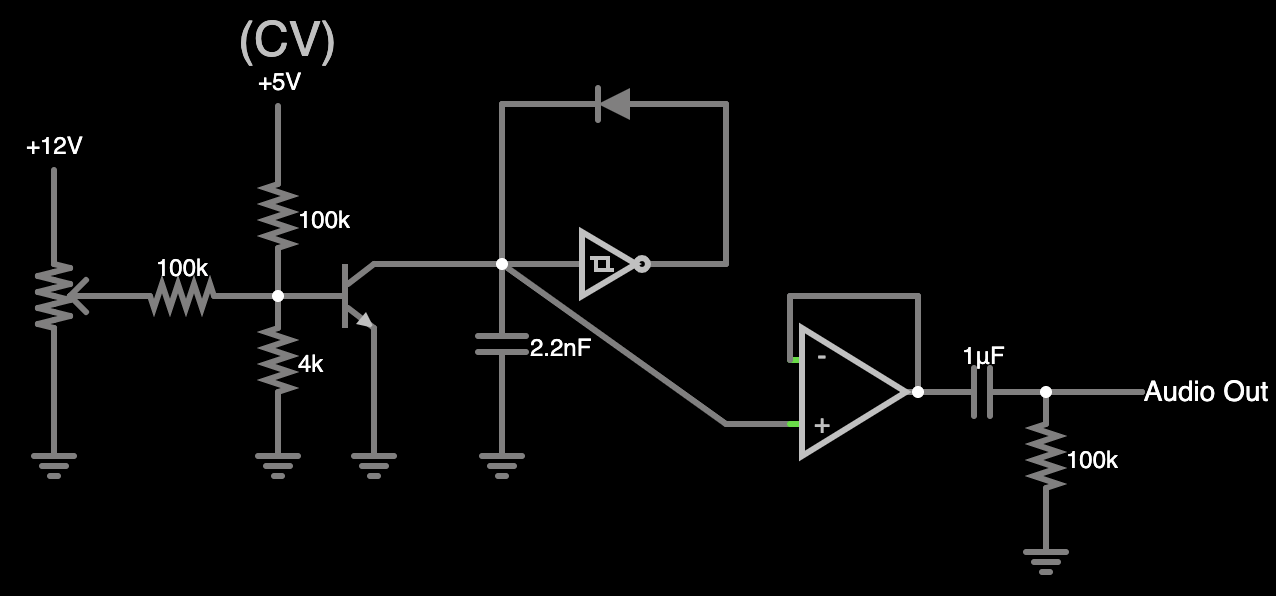
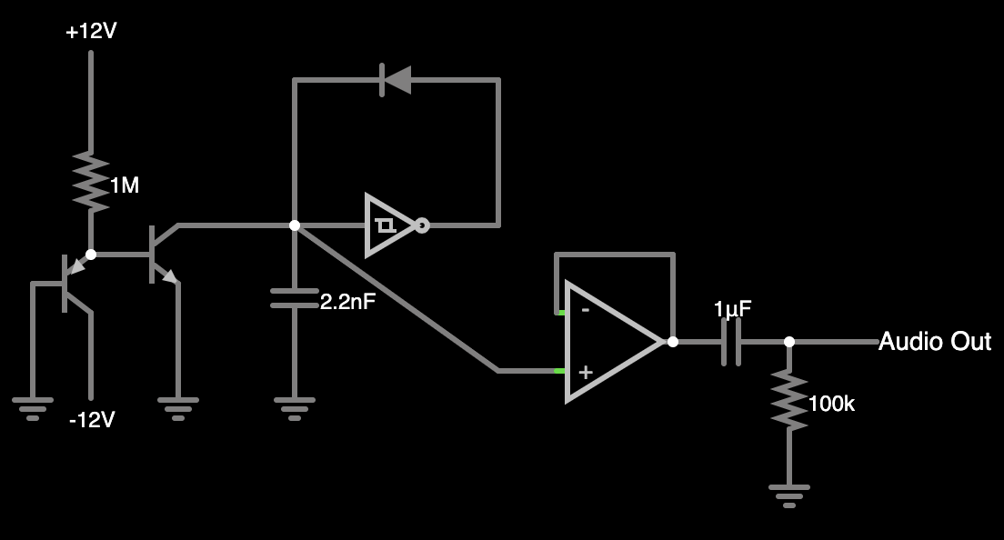
Changing the Frequency with a Voltage Control Input
Here we just add a jack and use a passive mixing circuit – nothing more than a couple of resistors – so that we can control the pitch with both an external CV input and the potentiometer from the previous step. Really, they’re both just sources of variable voltage. Finally we tie the output to ground with a 4 or 14k resistor to bring the sum down a bit.
Now here’s the schematic:
Deal with Component Temperature Variations
Having added a Control Voltage input in the previous step, we now must rip it out to add support for additonal components.
Because the NPN transistor warming lowers its resistance to ground, raising the pitch of the oscillator, we add a PNP transistor, which has the opposite effect when warmed. The idea here is that the two transistors will counteract each other (hopefully!), producing a mostly steady pitch once the oscillator is tuned. The base of the PNP transistor is connected to ground because – well, because it’s handy at the moment, really. This is not how we will have it long-term.
I really needed the schematic here:
One thing to point out here is that the PNP transistor’s collector is connected to -12V, not ground! This is on purpose as we are trying to keep the voltage at the emitter within the 0-550mV range that is appropriate for the NPN transistor’s base, as you can see from the schematic. Connecting the PNP transistor’s collector to -12V instead of ground does that.
Add Tuning
Now we add the tuning knob and CV input back into the circuit, also adding a fine tuning adjustment.
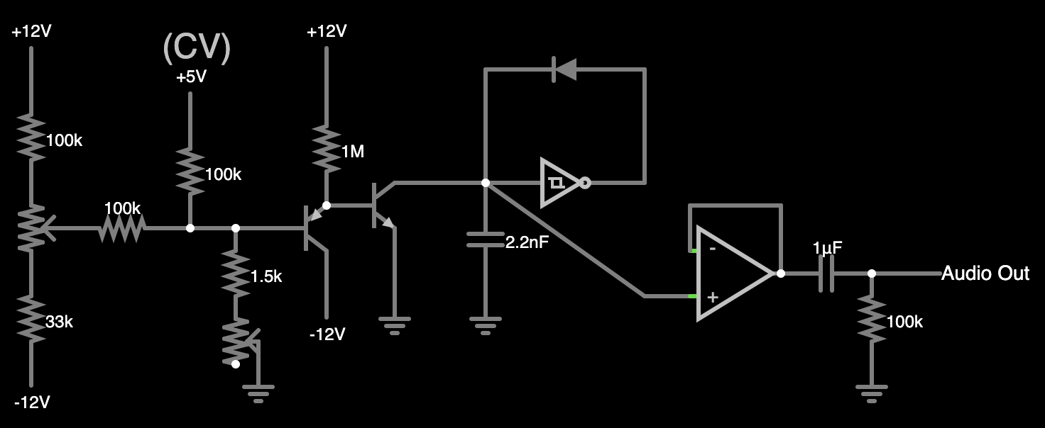
There’s a trim potentiometer which is connected to a 1.5kΩ resistor in the schematic, but I didn’t have any special symbol for that, so I just used a standard potentiometer symbol. That potentiometer is used for the oscillator’s fine tuning adjustment.
The biggest problem I had with building this part of the circuit was that I couldn’t find the trim pot. There’s about a 95% chance I lost it while digging through the bag for a diode. I picked one up from my local supplier at a price which bordered on highway robbery, but I don’t care, because I can’t tell you how nice it is to have an electronics parts store within a few blocks of my house and I would very much like them to remain in business.
The coarse tuning potentiometer has returned, now connected to -12V instead of ground. The oscillator has been fairly high-pitched, and the designer wants to bring the pitch down by lowering the voltage sent from the tuning potentiometer. How low?
The tuning potentiometer forms part of a voltage divider between the +12V and -12V supplies. The voltage divider output is:
| Potentiometer setting | Voltage divider calculation | Output |
|---|---|---|
| 0% | 24V * 100kΩ / (100kΩ+133kΩ) - 12V | -1.7V |
| 50% | 24V * 150kΩ / (150kΩ+83kΩ) - 12V | 3.4V |
| 100% | 24V * 200kΩ / (200kΩ+33kΩ) - 12V | 8V |
Compare that to the circuit in the “Changing the Frequency with a Voltage Control Input” section:
| Potentiometer setting | Voltage divider calculation | Output |
|---|---|---|
| 0% | 12V * 0kΩ / (0kΩ+100kΩ) | 0V |
| 50% | 12V * 50kΩ / (50+50kΩ) | 6V |
| 100% | 12V * 100kΩ / (100kΩ+0kΩ) | 12V |
So we can see that the voltage is indeed lower. More importantly, the range of the coarse tuning adjustment is now closer to a “musically useful” range, which is around 0-8V.
Add PWM Wave Shape
Other than the breadboard getting a bit crowded and the potentiometers not really fitting into the breadboard well as usual, this step went fairly easily.
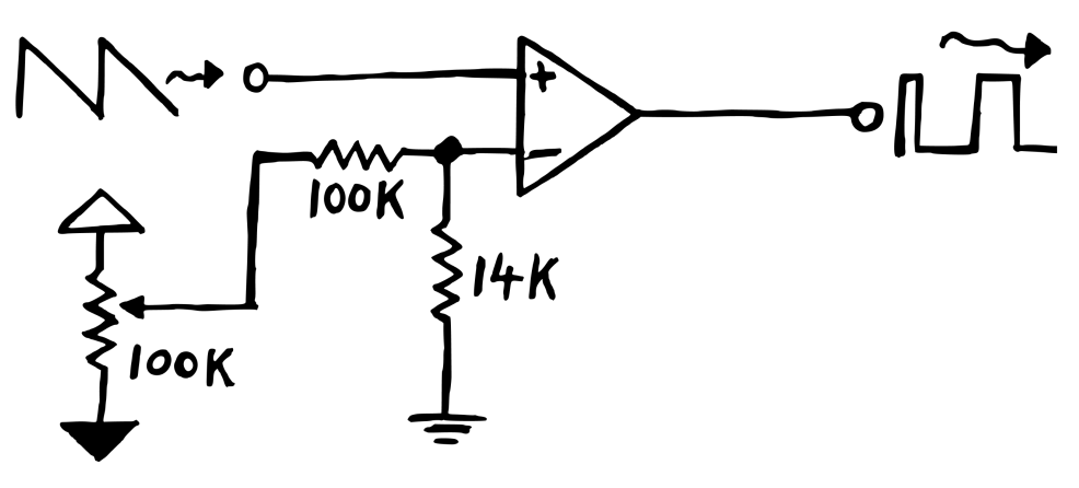
The general idea of this step is to use an op amp wired as a
comparator: a
circuit which returns a high voltage if the + input is higher than the - input
and a low voltage otherwise. Sending the sawtooth wave through such a circuit
results in a pulse wave which we can vary the width of by adjusting the voltage
going to the - input of the op amp.
I do find the explanation of using an op amp as a comparitor in the directions a bit confusing, however. I much prefer this version, from Make: Analog Synthesizers, by Ray Wilson:
Here we are applying a… voltage to the inverting input [
-] of the op amp, and the noninverting input [+] is the input to the comparator. If we apply a [lower voltage] to the noninverting input, the output of the op amp will go as low as it can. The op amp really wants to pump current away from the inverting input through the nonexistent feedback resistor. As long as the voltage on the noninverting input is lower than the voltage on the inverting input, the op amp’s output will remain saturated low (stuck at its maximum negative output voltage). If the voltage on the noninverting input goes above [the voltage on the inverting input], the output of the op amp will become saturated high (stuck at its maximum positive output voltage) again in a vain effort to pump current to the inverting input through the nonexistent feedback resistor.
In short, think of the op amp comparitor as a buffer with the feedback resistor set to infinity instead of nothing.
Add PWM Width Control
This is just a potentiometer voltage divider going into the inverting [-]
input of the comparitor op amp above.
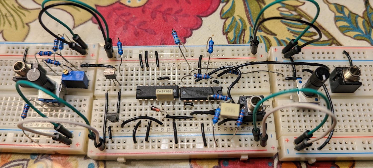
This pretty much just worked, although once again getting the potentiometer to stay in the breadboard was a bit fiddly. Also I ran out of room on the tiny breadboards I had, so I ended up daisy chaining three of them together. I have purchased a larger breadboard for the remaining kits.
Add Output Level Control
Here we add a couple of op amps to normalize both the sawtooth and the square wave outputs. Finally we can hear the square wave as the output is no longer so hot that it would damage your headphones if you connect it.
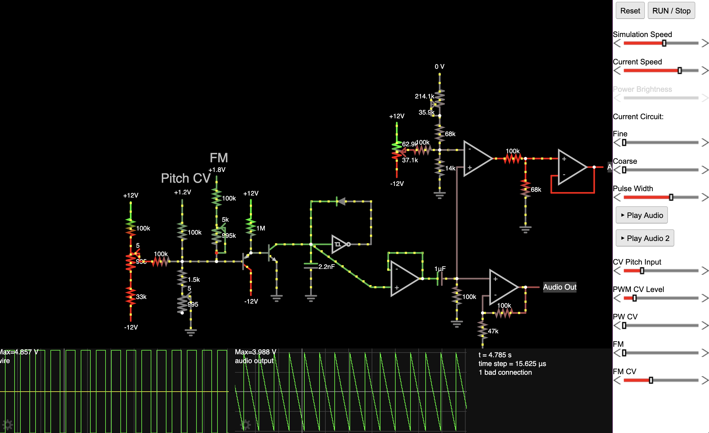
Here’s my final physical circuit:
Also, I made a simulation of the full VCO as built on the breadboard which I invite you to play with. You can interact with the simulation via the sliders on the right, and you can hear the oscillator by pressing the two “Play Audio” buttons.
Coming Soon!
Having built a working circuit, it’s now time to rip all of the components out of the breadboard and solder them (plus a few extras) onto the PC board. But before I do that, I’m going to take some time to explain how op amps work. Sorry, folks, that’s about as much of a cliffhanger as I can manage.
Resources
Instructions
Community
Product Pages
Simulation
- The VCO core
- VCO core with CV and tuning
- The full VCO (as breadboarded; this is missing a few components not on the breadboard such as thermistors and output protection resistors)
Videos
- Introducing the mki x es.edu DIY VCO kit by Moritz Klein (7:23). This is a super-short overview with a demo of the full system.
- DIY VCO Part 1: The analog oscillator core anyone can build, DIY VCO Part 2: The simplest exponential converter, DIY VCO Part 3: Tuning your VCO (and making sure it stays in tune), and DIY VCO Part 4: Shaping Sawtooth to Square. Four-video series by Moritz Klein, 1:02:00 all together. It’s important to note that in this series he builds a somewhat different VCO than the one which ships in the mks x es.EDU kit. But it has a lot in common and I still think this video series is very, very useful.